My DIY FPGA board can run Quake II (part 4)
22-Mar-2026
- Part 1/6: Introduction
- Part 2/6: First prototype
- Part 3/6: Now it mostly works
- Part 4/6: Next generation (you are here)
- Part 5/6: One more iteration
- Part 6/6: Optimizing hardware to run Quake II
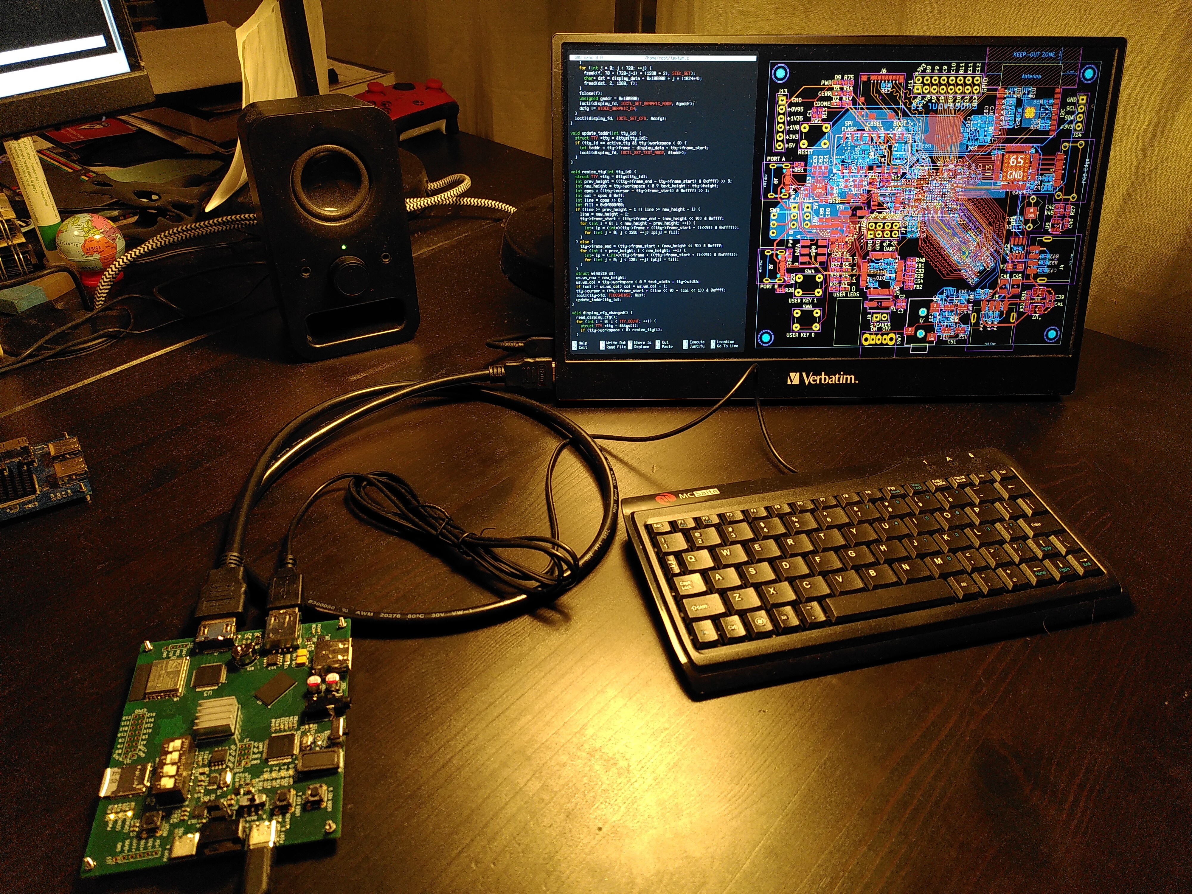
Time to design a new board
I didn’t want to simply recreate what I had before. Making something more advanced meant soldering BGA. I wasn’t sure if I could do it, but I decided to try anyway.
Specifically, I wanted a more advanced FPGA – I chose the Efinix Ti60F256 – and more modern memory – IM8G16D3FFBG, which is a 1GB DDR3L chip. The first has 256 pins and the second has 96, both with a 0.8 mm pitch.

Some IC in BGA-256 package. Not Ti60 though, but looks very similar.
After the struggles with DDR1, I had absolutely no desire to reinvent the memory controller. Fortunately, I found something with the promising name “DDR3 Soft Controller Core” on the Efinix website. On their community forum, I was also pointed to a guide on DDR3 PCB layout recommendations.
There were new unfamiliar terms, so I had to spend more time diving into the theory.
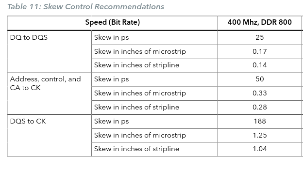
I barely managed to meet the trace length matching requirements. The recommendations also suggested routing all address and command lines on a single layer, but that seemed impossible. Instead, I tried to account for the difference in signal propagation speeds across different layers and compensated by shortening the traces on the internal layer.
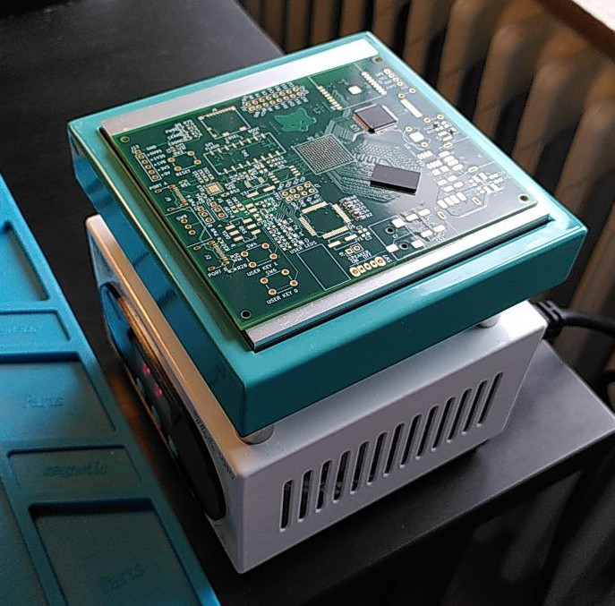
This time the PCB has 6 layers
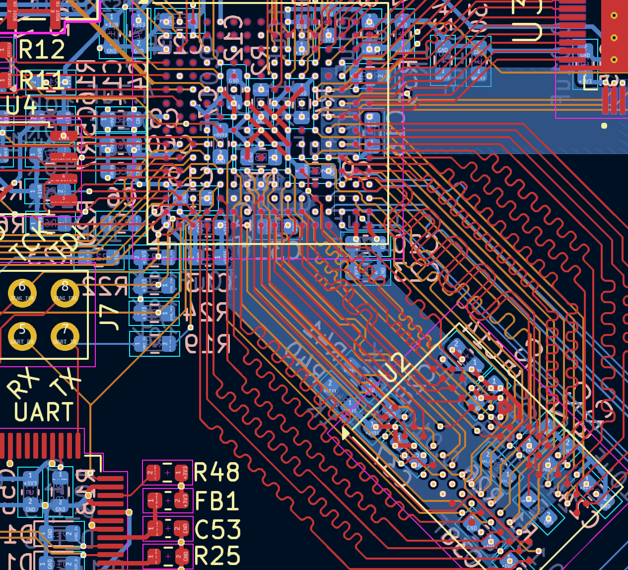
I studied the recommendations for the quantity and values of the decoupling capacitors on the power inputs. However, I still couldn’t follow them strictly; that many components simply wouldn’t fit physically near the power pins, and I really didn’t want to solder anything smaller than 0603 (i.e. 0.06” x 0.03” — 1.6 x 0.8 mm). I just squeezed in as many as I could.
Capacitors on the back of the board under FPGA, 3d model
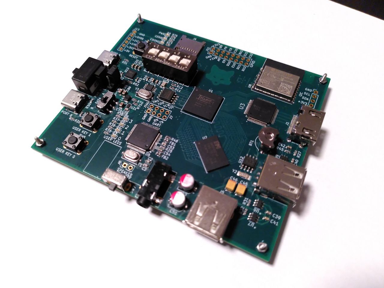
Other changes compared to the previous board:
- A separate TMDS serializer chip (TFP410) to avoid those green artifacts.
- A current limiter for connected USB devices.
- The ability to switch the SD card data line voltage from 3.3V to 1.8V. Potentially, this allows to increase the data transfer speed to 104 MB/s (UHS-1 SDR104 mode).
- A real-time clock and a battery, so that Linux doesn’t find itself in 1970 every time it boots.
- An ESP32 module to serve as a WiFi adapter.
- In case the standard 500mA at 5V from USB is insufficient, I added a second USB-C port and a chip capable of requesting a higher voltage from the power supply.
How to solder BGA
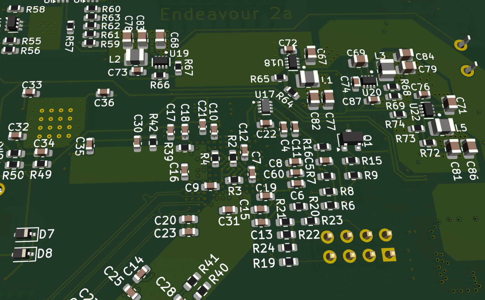
As it turns out, ordering a six-layer PCB from JLCPCB is significantly more expensive than a two-layer one. This time, the total came to over $100, and the price was nearly the same whether I ordered 5, 10, or 20 copies. For comparison, my previous batch of five two-layer boards cost only $2.
PCBs and stencil; previous PCB is added for comparison (bottom right)
Most articles found when searching for “how to solder BGA” are about repairs. Heating with a heat gun, removing a chip from one device, cleaning off the old solder, reballing (placing a solder ball on every pad), and soldering it onto the device being repaired. This is quite difficult and requires specific equipment, but fortunately, it isn’t necessary in this case.
Soldering new chips onto new devices is much easier. First, apply solder paste to all the contact pads on the board. Then, place the chips on top and heat them. Note: The solder paste must be rated for the same temperature as the solder balls on the chip’s pads. If you’re lucky, everything will solder where it should without any bridging where it shouldn’t, and you’re done. If something goes wrong, which may not be visible, scrap it and start over (or refer to the paragraph above about repairs).
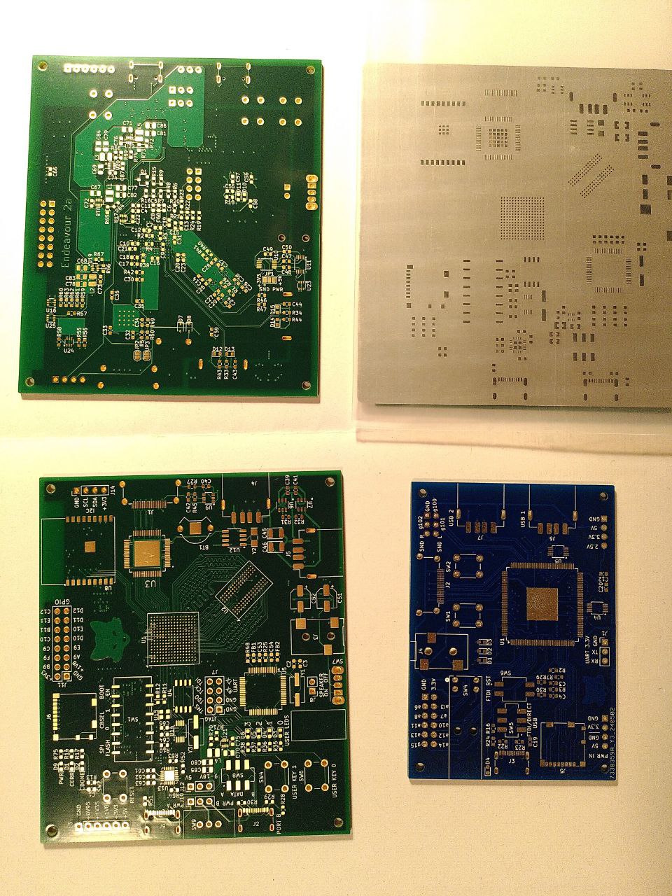
To apply the solder paste neatly, a stencil is needed. My stencil (ordered along with the board) has width exactly matching the size of the PCB. This is quite important, as it makes it easier to align with the board. I used a duct tape to secure the stencil and a plastic card to spread the paste.
I bought a bottom heater with adjustable temperature, listed on the store’s website as a “Uyue 946 Constant Temperature Heating Station Screen Removal tool”. Before getting down to business, I practiced (I have plenty of spare PCBs) on several cheaper memory chips bought specifically for this purpose. I heated a test sample to 221°C and watched the solder paste change color and form into balls.
Bottom heater
I examined the resulting balls on the FPGA footprint. No defects were visible, so I could move on.
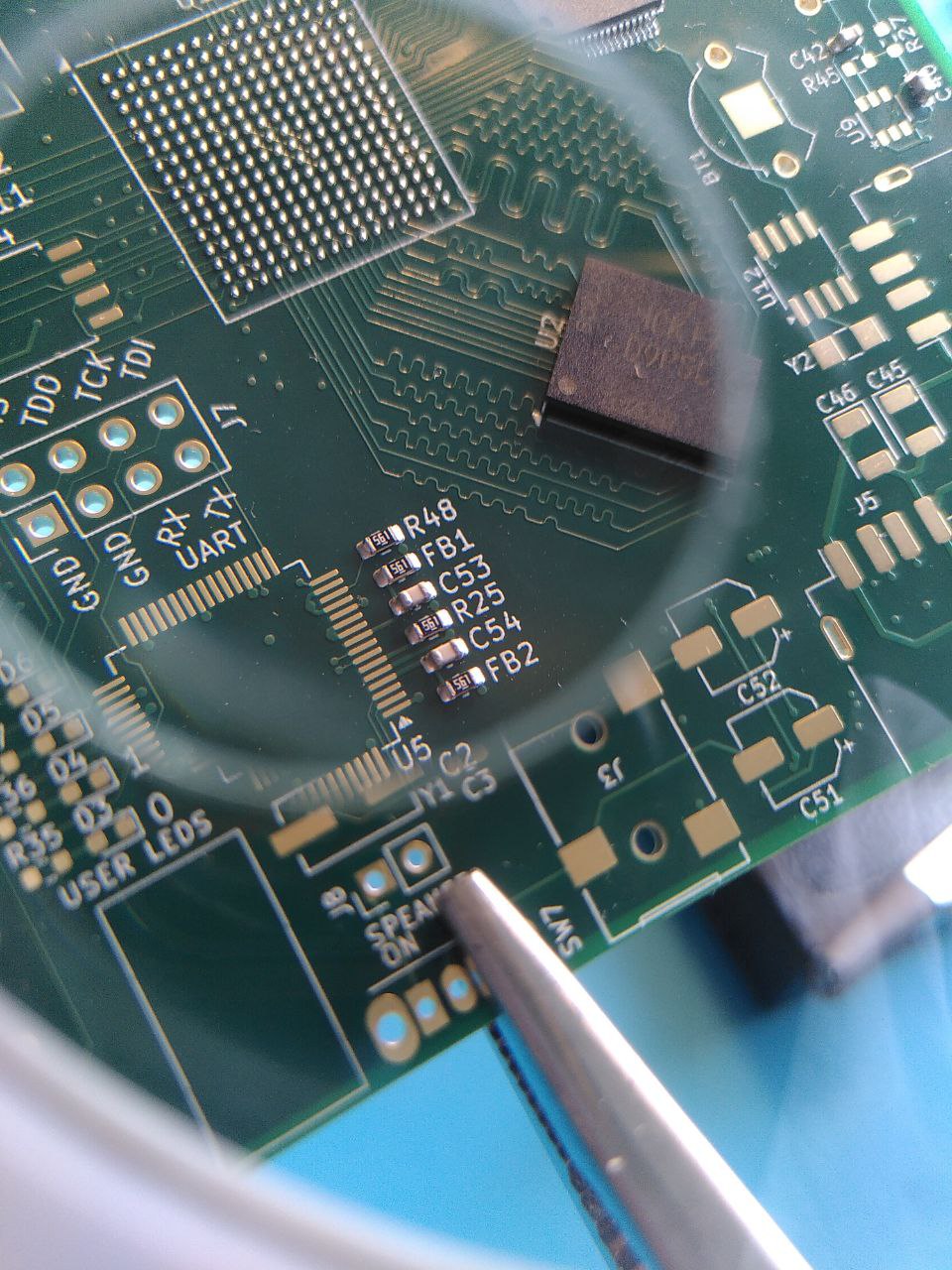
Test run
With a bottom heater, one can only solder the components on the top side of the board. Then, dozens of capacitors and resistors need to be added to the bottom without damaging anything on the other side. I decided to solder the bottom side with a heat gun and, just in case, used solder paste with a lower melting point (183°C).
Surprisingly, everything worked on the first try. The first try took three days: soldering the top side, the bottom side, and then the connectors separately. There were no significant issues. In a couple of places adjacent pins bridged (luckily not under the BGA chips), but I managed to separate them.
Well, “everything worked” is a bit of an exaggeration. After a few months of writing and debugging drivers, I discovered that the Wi-Fi wasn’t working because I had used the wrong pins on the ESP32 module, which caused a delay in SPI transfers. This issue has been resolved in the next revision of the board, I’ll come to it later.
System on Chip
A System on a Chip (SoC) is an integrated circuit that consolidates all essential computer components — including the CPU, memory, graphics (GPU), and I/O interfaces — onto a single chip.
The term “FPGA” stands for “field-programmable gate array” meaning the chip can be programmed to perform any custom digital logic. This custom digital logic (which in my case is a complete SoC) must be defined using a hardware description language (HDL). The most common HDLs are Verilog and VHDL. HDL code essentially describes how logic elements, such as AND, OR, and NOT, should be connected to each other.
On this scheme the SoC is what is inside the big green rectangle “FPGA Ti60”. Other green rectangles are other chips on the board.
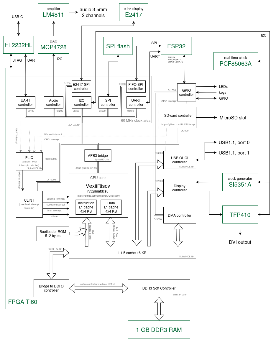
All the components on the scheme with no marked source are designed by me and available on my github (Verilog code, Scala code). DDR3 Tilelink adapter, UART controller, I2C controller, audio controller, SPI controllers (SPI FLASH, ESP32 SPI, and E2417 SPI interfaces have different requirements, so I ended up with 3 different SPI controllers optimized for specific use cases), etc. Most notable are video controller and DMA controller.
The most complicated part of a SoC is, of course, the processor core. And I didn’t do one on my own.
I used the following IP cores:
- VexiiRiscv — RISC-V core written in SpinalHDL.
- A few components distributed with SpinalHDL including Tilelink interconnect, APB3 bridge, USB OHCI controller, PLIC.
- ZipCPU/sdspi SD-Card controller.
- Efinix DDR3 Soft Controller Core (source not available, can be used only with Efinix FPGAs).
I must say that VexiiRiscv and SpinalHDL (both created by Dolu1990) are incredibly impressive. These projects are far more advanced than anything I could write in HDL on my own.
When I started my project, I preferred Verilog and only used SpinalHDL to generate a Verilog module from VexRiscv’s Scala sources. Over the last two years, however, I have used SpinalHDL more and more, and now I even prefer it to Verilog when writing my own modules.
The learning curve was not easy though. SpinalHDL is a set of libraries that generate Verilog/VHDL code from Scala. It becomes quite tricky when hardware abstractions (pipelines, finite-state-maschines, busses, caches — CPU is not a simple thing) and generation-time stuff (coroutines, delayed instantiation, inheritance, plugins) are mixed in a single file.
Also I was new to Scala and often couldn’t tell if a sequence of characters was a variable name or something defined deep within SpinalHDL’s internals or just standard Scala syntax (I remember googling what "???" means in Scala; Google ignored the question marks assuming that I just ask with a lot of expression).
The documentation is well-written, but doesn’t cover everything. I would definitely buy a 1,000-page book like “Basics of SpinalHDL” or “Learn SpinalHDL in 21 Days” if somebody wrote one.
Fortunately Dolu1990 was always ready to answer questions (Dolu1990, if you read this, thank you!!!).
Results
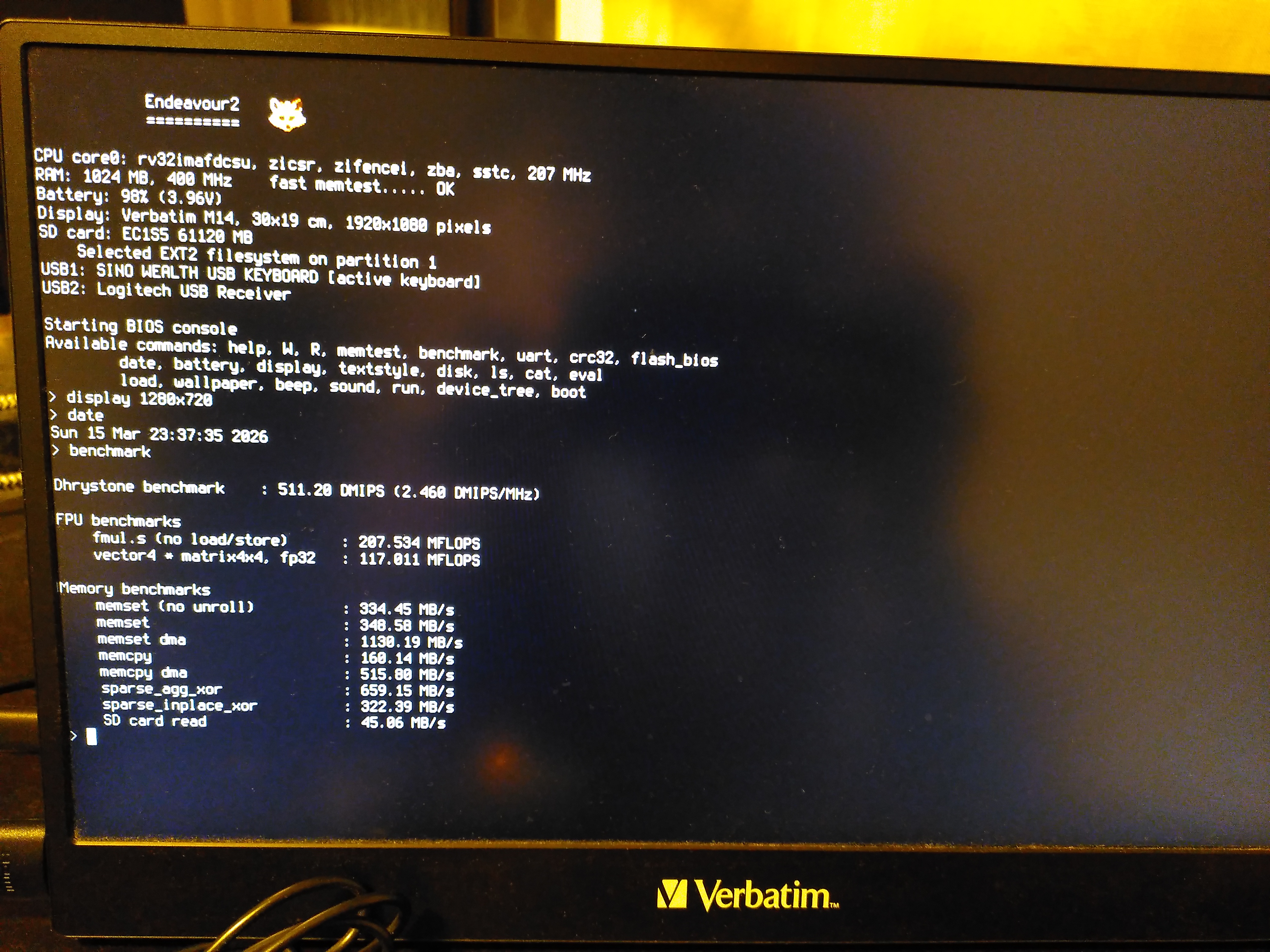
- FPGA utilization: 53612/60800 XLRs (89%), 241/256 memory blocks (95%).
- Single riscv32 core (two cores could fit into design only if I sacrifice FPU) working at 207 MHz.
- Dhrystone benchmark: 511 DMIPS (2.46 DMIPS/MHz). It is more than Pentium, but a bit less than Pentium II.
- 1 GB RAM — more than an average Pentium II PC could hope for.
- Floating-point benchmark: peak 207 MFLOPS (or 117 MFLOPS on a more realistic benchmark).
- Coremark 1.0: 783.08.
- SD card read: 45.06 MB/s.
- CPU memset: 348 MB/s.
- DMA memset: 1130 MB/s (theoretical hardware limit is 1.6 GB/s if we assume data transfer on every single tick).
I’ll say more about DMA when I get to optimizing Quake II. I wanted to implement a GPU, but I was limited by the remaining FPGA resources. So, I created a “DMA controller” that can also perform a few graphics-related operations.
And a few screenshots
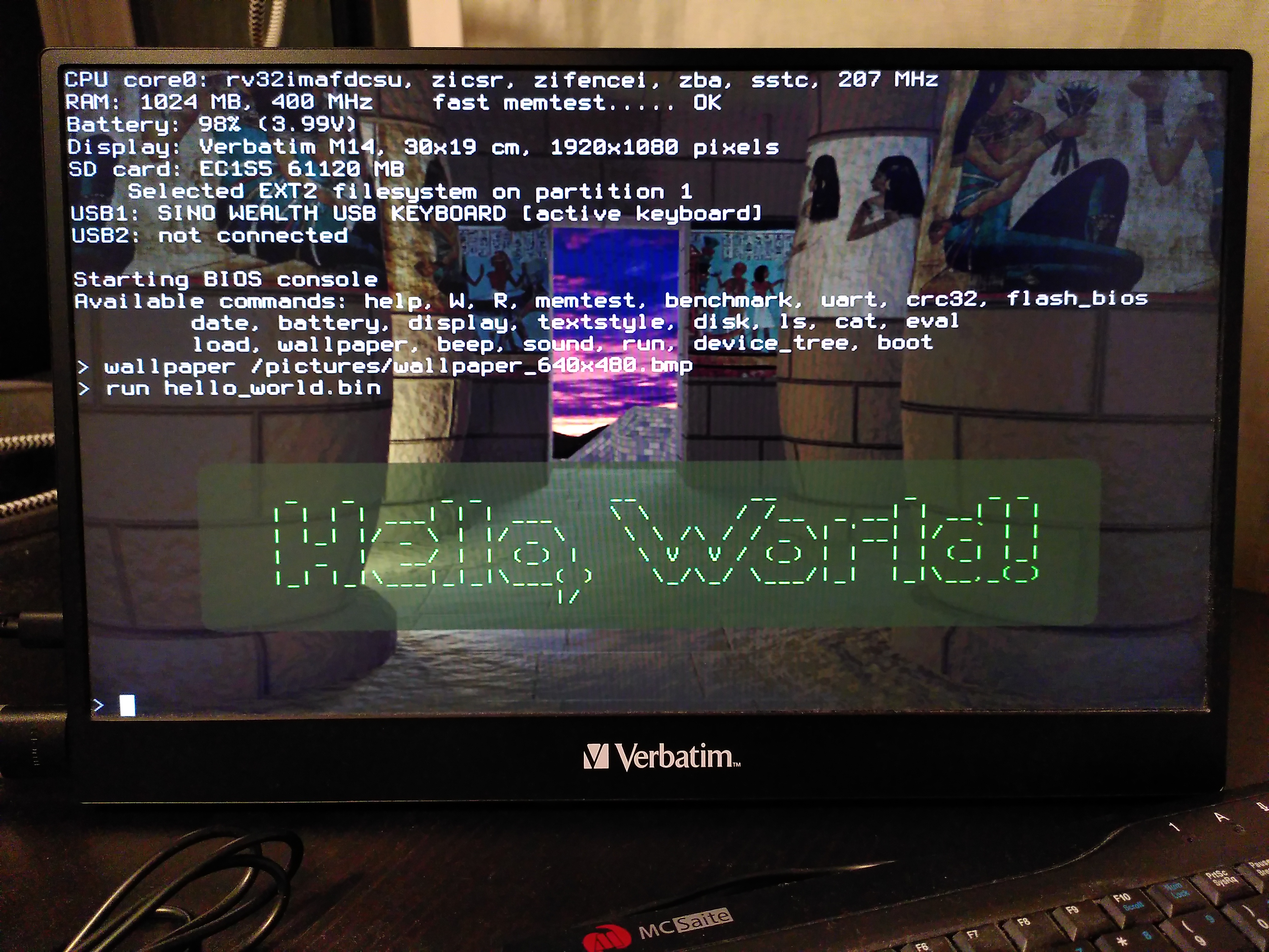
Bare metal Hello World
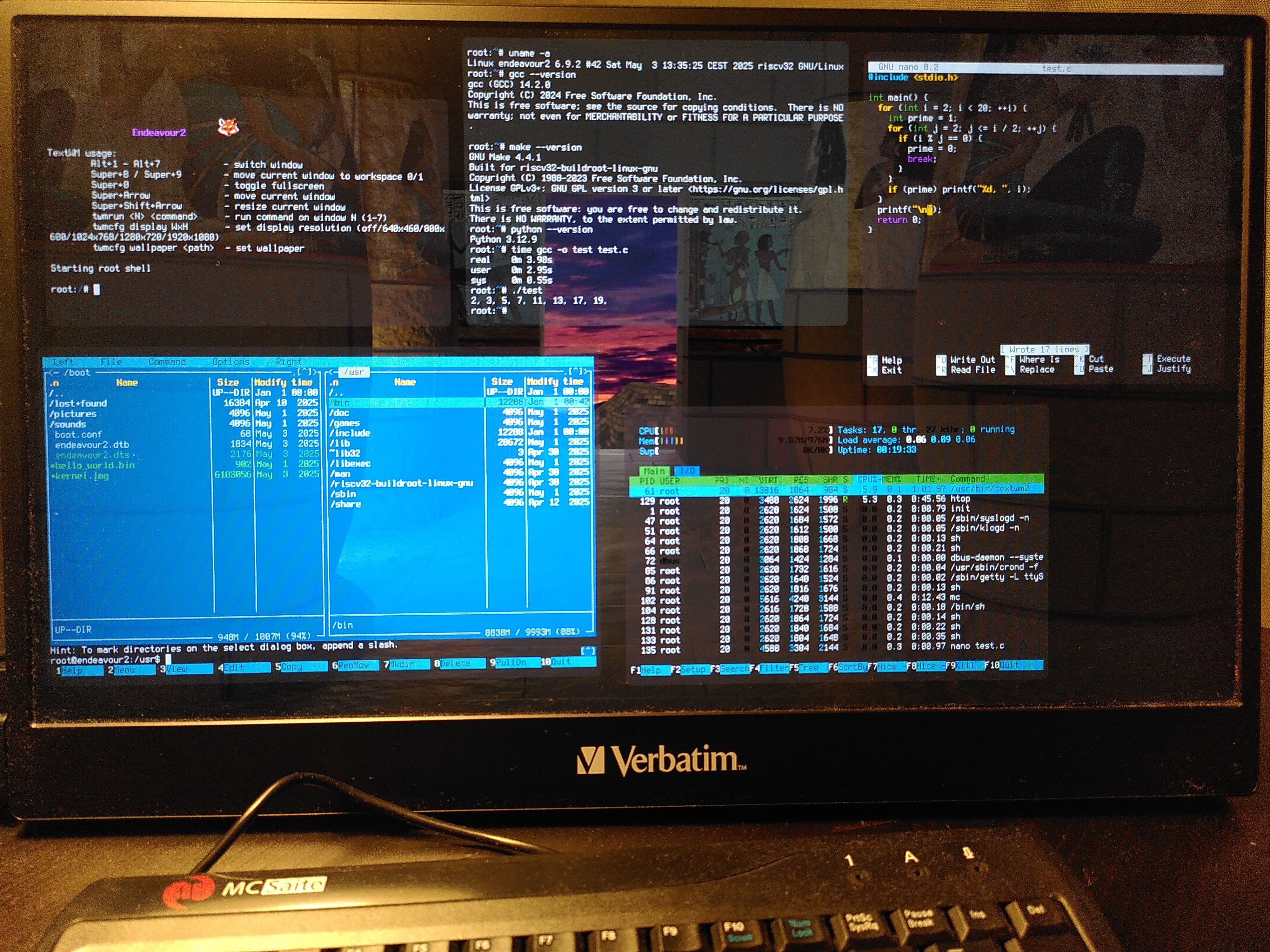
My window manager and TTY implementation
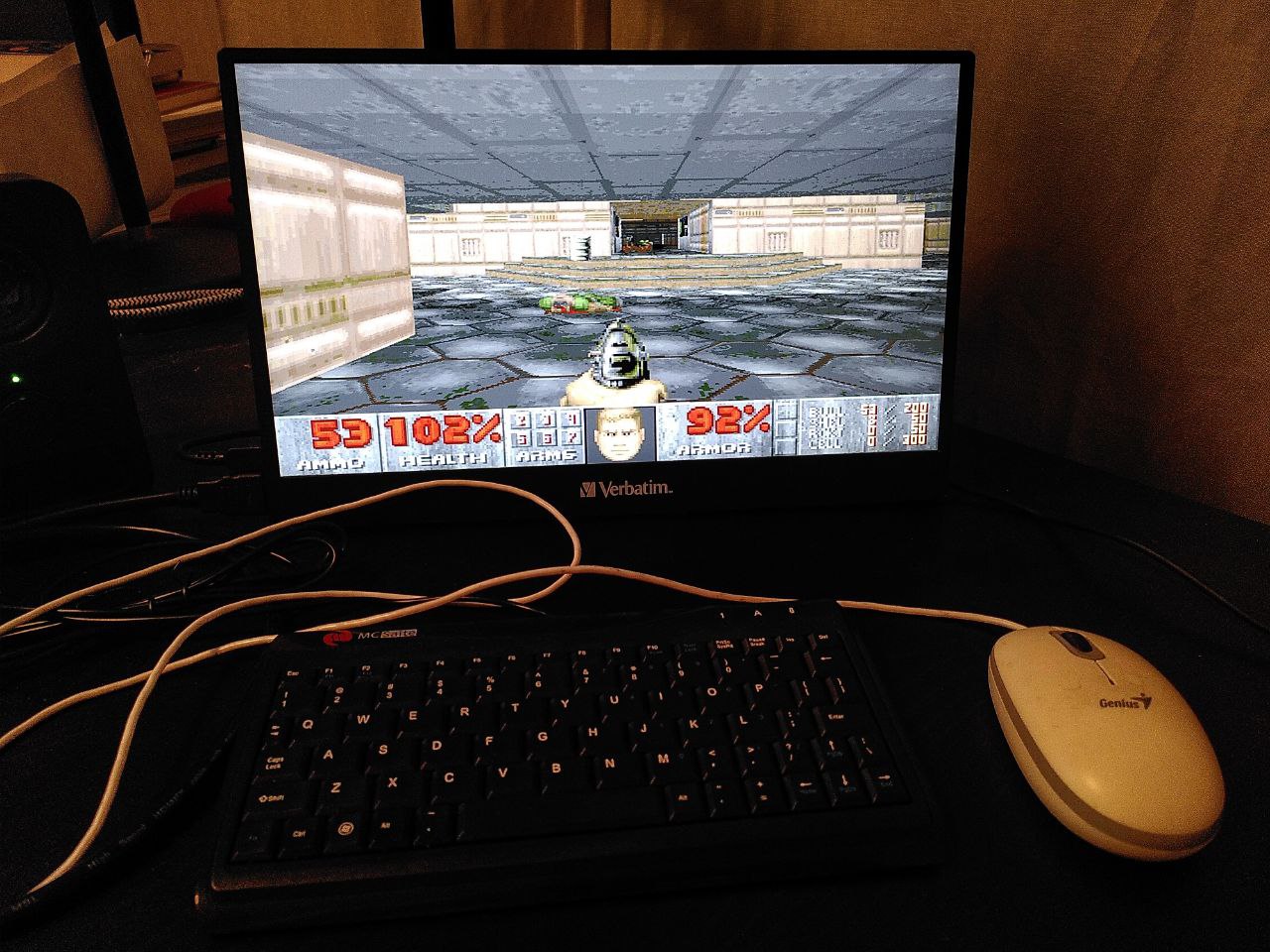
Doom
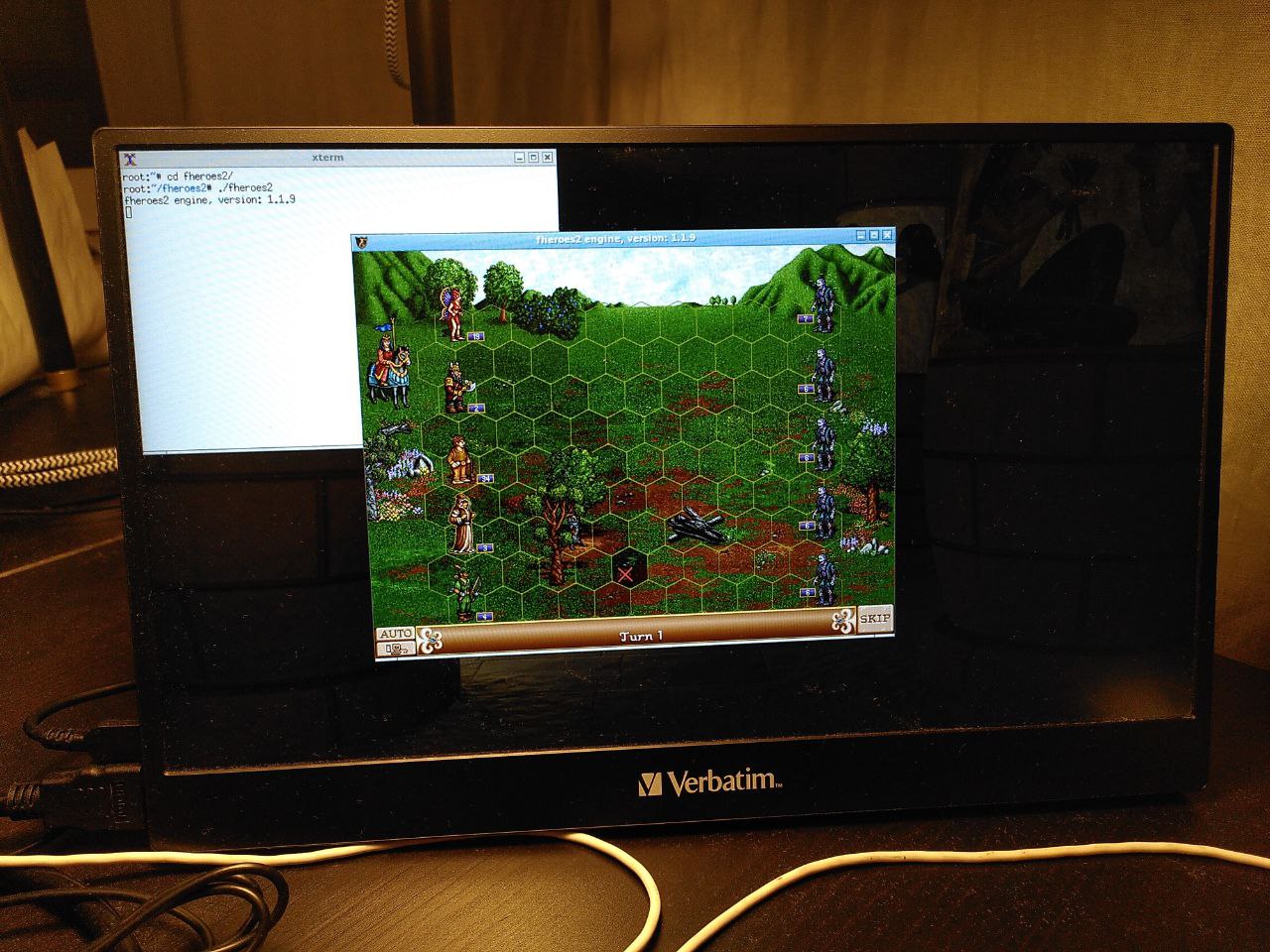
Heroes2
More pictures in the next part.
Next part: One more iteration (5/6)